Schematic 555 Timer Circuit Diagram : The 555 Timer In Astable Mode Youtube / Generally, it's miles a monolithic timing circuit that offers unique and surprisingly stable delays of time or oscillation.
Schematic 555 Timer Circuit Diagram : The 555 Timer In Astable Mode Youtube / Generally, it's miles a monolithic timing circuit that offers unique and surprisingly stable delays of time or oscillation.. Lm555 interlocked timers schematic normal triggering and timing lengths are not affected by this method. Print the diagram in the centre of a sheet of paper create a circuit using the ics pin locations. The circuit may be triggered and reset on falling waveforms, and the output circuit can source or sink up to 200ma or drive ttl circuits. Finally, power up your circuit by connecting the battery to your breadboard Pinout diagram and different modes of operations, applications, features, example circuit simulations, datasheet.
By adding one or two external resistors and one capacitor the. Reset and control input terminal. However, d1 may be eliminated if we. The schematic diagram of the soft start system is shown in figure. This tutorial provides sample circuits to set up a 555 timer in monostable, astable, and bistable modes as well as an in depth discussion of how the by wiring the 555 timer with resistors and capacitors in various ways, you can get it to operate in three different modes:
Monstable Multivibrator Using 555 Timer from electrosome.com Reset and control input terminal. Finally, power up your circuit by connecting the battery to your breadboard The second circuit adds d1 to the emitter of q1 in order to increase vebo. The 555 timer circuit of fig. If you force the timer input to stay low past timeout the output will stay. The 555 timer ic becomes invented via signetic organization and it becomes termed as se or ne555 timer. 5.32 that should still be working will be used as the clock signal to drive the now the schematic symbol and pcb symbol are created for the 555 timer. Lm555 timer internal circuit block diagram.
The timer will start when the wire is inserted into the protoboard between these two points, and ignore further contacts. Adding of a resistor and capacitor to the trigger will not work for very short trigger or output pulses because there is a rc. The block diagram of a 555 timer is shown in the above figure. An external triggering is required for transition from stable to unstable state. Print the diagram in the centre of a sheet of paper create a circuit using the ics pin locations.
Comparing 555 Pwm Circuits General Electronics Arduino Forum from aws1.discourse-cdn.com Look at the circuit diagram. The 555 timer can provide time delays ranging from several minutes for one cycle of operation to many thousands of cycles per second. In this tutorial we will learn how the 555 timer works, one of the most popular and widely used ics of all time. Print the diagram in the centre of a sheet of paper and then draw a circuit using the ics pin locations. 555 timer ic remains in stable state until the external triggering is applied. This is one of the most basic 555 circuits. Monostable mode is great for creating. Generally, it's miles a monolithic timing circuit that offers unique and surprisingly stable delays of time or oscillation.
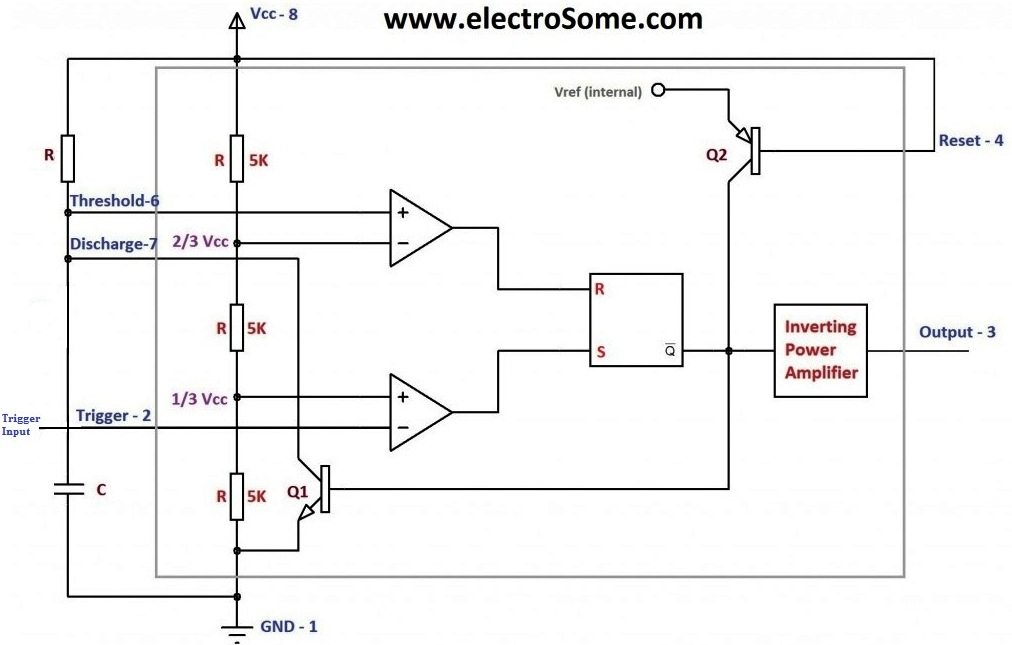
555 timer construction & block diagram 555 timer pinout configuration schematic & working principle of 555 timer 555 timer internal function timers are those circuits, which provide periodic signals to a digital system which change the state of that system.
A 555 timer has two comparators, which are. Some important features of the 555 timer: Generally, it's miles a monolithic timing circuit that offers unique and surprisingly stable delays of time or oscillation. The output of uc (upper comparator) which is reset input to rs latch is high when the threshold input is high or. The 555 timer circuit of fig. 555 timer construction & block diagram 555 timer pinout configuration schematic & working principle of 555 timer 555 timer internal function timers are those circuits, which provide periodic signals to a digital system which change the state of that system. Lm555 timer internal circuit block diagram. The 555 and 7555 are called timers or timer chips. The 555 timer ic becomes invented via signetic organization and it becomes termed as se or ne555 timer. The block diagram of a 555 timer is shown in the above figure. The schematic shows (3) circuits, because one circuit does not work well over the entire vcc range. The schematic diagram of the soft start system is shown in figure. The circuit may be triggered and reset on falling waveforms, and the output circuit can source or sink up to 200ma or drive ttl circuits.
The block diagram of a 555 timer is shown in the above figure. Derivatives provide two (556) or four (558) timing circuits in one package. The primary purpose of the 555 timer is the generation of accurately timed single pulse or oscillatory pulse waveforms. Print the diagram in the centre of a sheet of paper and then draw a circuit using the ics pin locations. The circuit inside the 555 is just an amplifier with 2 inputs and an output.
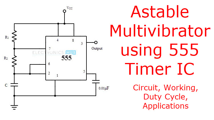
Astable Multivibrator Utilizing 555 Timer Circuit Obligation Cycle Purposes Electrician World News from www.electronicshub.org The 555 timer ic is an integrated circuit (chip) used in a variety of timer, delay, pulse generation, and oscillator applications. The circuit inside the 555 is just an amplifier with 2 inputs and an output. Above schematic diagram shows the 555 timer monostable multivibrator circuit. A 555 timer has two comparators, which are. The 555 can be used to provide time delays, as an oscillator, and as a flip flop element. 5.32 that should still be working will be used as the clock signal to drive the now the schematic symbol and pcb symbol are created for the 555 timer. In other words, those circuits. Print the diagram in the centre of a sheet of paper create a circuit using the ics pin locations.
Reset and control input terminal.
555 timer construction & block diagram 555 timer pinout configuration schematic & working principle of 555 timer 555 timer internal function timers are those circuits, which provide periodic signals to a digital system which change the state of that system. Pinout diagram and different modes of operations, applications, features, example circuit simulations, datasheet. The schematic shows (3) circuits, because one circuit does not work well over the entire vcc range. Above schematic diagram shows the 555 timer monostable multivibrator circuit. Monostable mode is great for creating. The 555 can be used to provide time delays, as an oscillator, and as a flip flop element. If you see the internal block diagram of 555 timer ic then it consists of the following parts. Print the diagram in the centre of a sheet of paper and then draw a circuit using the ics pin locations. The 555 timer is an integrated circuit, it is extremely versatile and can be used to build lots of different circuits. Lm555 interlocked timers schematic normal triggering and timing lengths are not affected by this method. The circuit may be triggered and reset on falling waveforms, and the output circuit can source or sink up to 200ma or drive ttl circuits. • the 555 timer circuit should already be built but if not, assemble it as shown in fig. This consists of a few different elements:
The block diagram of a 555 timer is shown in the above figure 555 timer schematic. This tutorial provides sample circuits to set up a 555 timer in monostable, astable, and bistable modes as well as an in depth discussion of how the by wiring the 555 timer with resistors and capacitors in various ways, you can get it to operate in three different modes:


0 Komentar